- 您现在的位置:买卖IC网 > Sheet目录2008 > MAX1394ETB+T (Maxim Integrated Products)IC ADC 8BIT 416KSPS 10-TDFN-EP
MAX1391/MAX1394
4
_______________________________________________________________________________________
1.5V to 3.6V, 416ksps, 1-Channel True-Differential/
2-Channel Single-Ended, 8-Bit, SAR ADCs
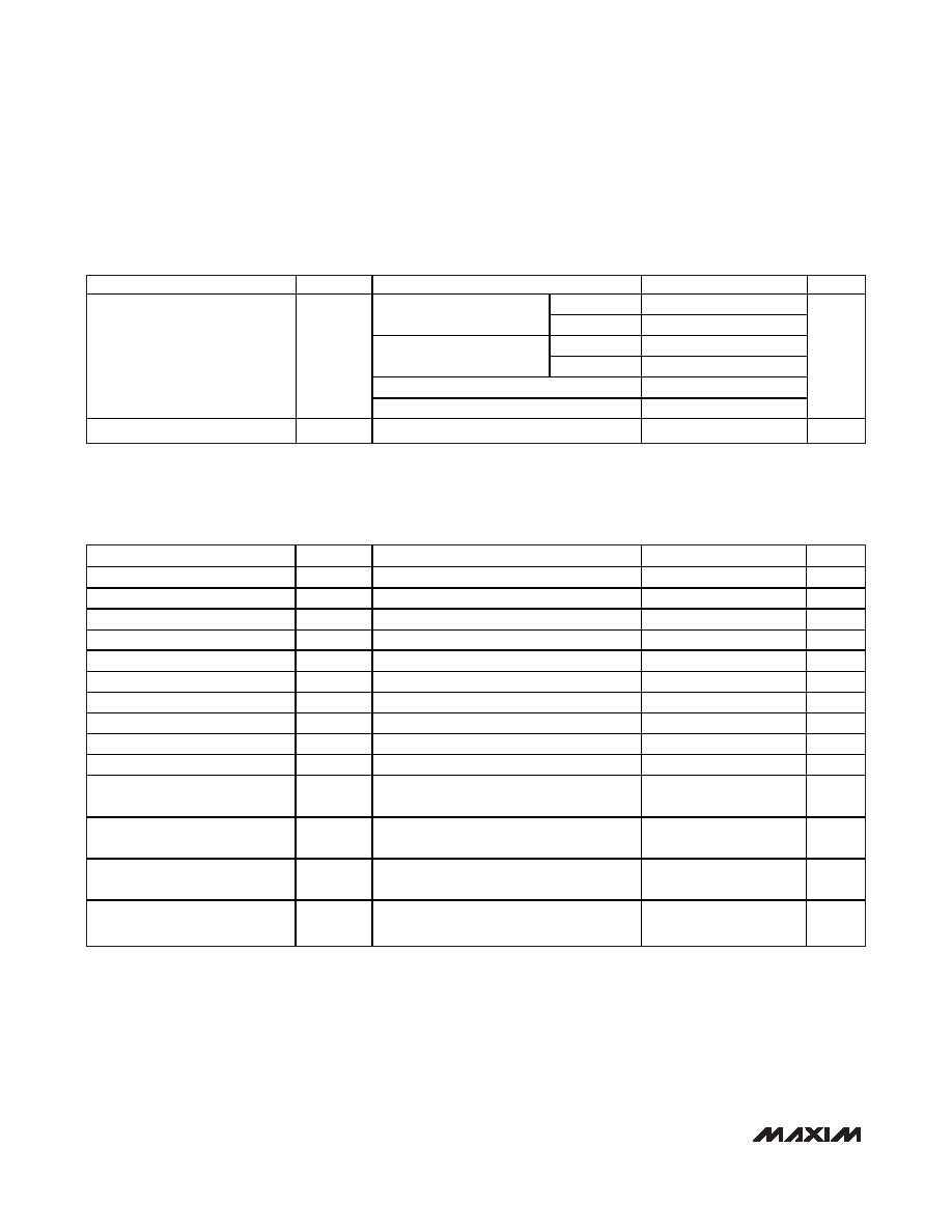
ELECTRICAL CHARACTERISTICS (continued)
(VDD = +1.5V to +3.6V, VREF = VDD, CREF = 0.1F, fSCLK = 5MHz, TA = TMIN to TMAX, unless otherwise noted. Typical values are at
TA = +25°C.) (Note 1)
PARAMETER
SYMBOL
CONDITIONS
MIN
TYP
MAX
UNITS
VDD = 1.6V
125
150
fSAMPLE = 100ksps
VDD = 3V
150
200
VDD = 1.6V
520
600
fSAMPLE = 416ksps
VDD = 3V
710
800
Power-down mode (Note 5)
5
10
Positive Supply Current (Note 4)
IDD
Power-down mode (Note 6)
0.2
±2.5
A
Power-Supply Rejection
PSR
VDD = 1.6V to 3.6V, full-scale input (Note 7)
±150
±1000
V/V
TIMING CHARACTERISTICS
(VDD = +1.5V to +3.6V, VREF = VDD, CREF = 0.1F, fSCLK = 5MHz, TA = TMIN to TMAX, unless otherwise noted. Typical values are at
TA = +25°C.) (Figure 1)
PARAMETER
SYMBOL
CONDITIONS
MIN
TYP
MAX
UNITS
SCLK Clock Period
tCP
200
10,000
ns
SCLK Pulse-Width High
tCH
90
ns
SCLK Pulse-Width Low
tCL
90
ns
CS Fall to SCLK Rise Setup
tCSS
80
ns
SCLK Rise to CS Fall Ignore
tCSO
0ns
SCLK Fall to DOUT Valid
tDOV
CLOAD = 0 to 30pF
10
80
ns
OE Rise to DOUT Disable
tDOD
620
ns
OE Fall to DOUT Enable
tDOE
920
ns
CS Pulse-Width High and Low
tCSW
80
ns
OE Pulse-Width High and Low
tOEW
80
ns
CH1/CH2 Setup Time (to the First
SCLK)
tCHS
MAX1394 only
10
ns
CH1/CH2 Hold Time (to the First
SCLK)
tCHH
MAX1394 only
0
ns
UNI/BIP Setup Time (to the First
SCLK)
tUBS
MAX1391 only
10
ns
UNI/BIP Hold Time (to the First
SCLK)
tUBH
MAX1391 only
0
ns
Note 1: Devices are production tested at room and +85°C. Specification to -40°C are guaranteed by design.
Note 2: VDD = 1.6V, VREF = 1.6V, and VAIN = 1.6V.
Note 3: VDD = 1.6V, VREF = 1.6V, VAIN = 1.6VP-P, fSCLK = 5MHz, fSAMPLE = 416ksps, and fIN (sine wave) = 100kHz.
Note 4: All digital inputs swing between VDD and GND. VREF = VDD, fIN = 100kHz sine wave, VAIN = VREFP-P, CLOAD = 30pF on DOUT.
Note 5: CS = VDD, OE = UNI/BIP = CH1/CH2 = VDD or GND, SCLK is active.
Note 6: CS = VDD, OE = UNI/BIP = CH1/CH2 = VDD or GND, SCLK is inactive.
Note 7: Change in VAIN at code boundary 254.5.
发布紧急采购,3分钟左右您将得到回复。
相关PDF资料
MAX1395ETB+T
IC ADC 10BIT 357KSPS 10-TDFN
MAX1400CAI+
IC ADC 18BIT LP 28-SSOP
MAX1401CAI+
IC ADC 18BIT LP 28-SSOP
MAX1415AEWE+T
IC ADC 16BIT DELTA SIGMA 16-SOIC
MAX1421CCM+D
IC ADC 12BIT 40MSPS 48LQFP
MAX1426EAI+T
IC ADC 10BITS 10MSPS 28SSOP
MAX1434ECQ+D
IC ADC 10BIT 50MSPS 100-TQFP
MAX1444EHJ+T
IC ADC 10BIT 40MSPS 32-TQFP
相关代理商/技术参数
MAX1394ETB-T
功能描述:模数转换器 - ADC RoHS:否 制造商:Texas Instruments 通道数量:2 结构:Sigma-Delta 转换速率:125 SPs to 8 KSPs 分辨率:24 bit 输入类型:Differential 信噪比:107 dB 接口类型:SPI 工作电源电压:1.7 V to 3.6 V, 2.7 V to 5.25 V 最大工作温度:+ 85 C 安装风格:SMD/SMT 封装 / 箱体:VQFN-32
MAX1394MTB+T
功能描述:模数转换器 - ADC 8-Bit 2Ch 400ksps 3.6V Precision ADC RoHS:否 制造商:Texas Instruments 通道数量:2 结构:Sigma-Delta 转换速率:125 SPs to 8 KSPs 分辨率:24 bit 输入类型:Differential 信噪比:107 dB 接口类型:SPI 工作电源电压:1.7 V to 3.6 V, 2.7 V to 5.25 V 最大工作温度:+ 85 C 安装风格:SMD/SMT 封装 / 箱体:VQFN-32
MAX1394MTB-T
功能描述:模数转换器 - ADC RoHS:否 制造商:Texas Instruments 通道数量:2 结构:Sigma-Delta 转换速率:125 SPs to 8 KSPs 分辨率:24 bit 输入类型:Differential 信噪比:107 dB 接口类型:SPI 工作电源电压:1.7 V to 3.6 V, 2.7 V to 5.25 V 最大工作温度:+ 85 C 安装风格:SMD/SMT 封装 / 箱体:VQFN-32
MAX1395ETB
制造商:Maxim Integrated Products 功能描述:1.5V-3.6V357KSPS1-CHANNEL TRUE-DI - Rail/Tube
MAX1395ETB+
制造商:Maxim Integrated Products 功能描述:ADC SGL SAR 357KSPS 10-BIT SERL 10TDFN EP - Rail/Tube
MAX1395ETB+T
功能描述:模数转换器 - ADC 10-Bit 2Ch 357ksps 3.6V Precision ADC RoHS:否 制造商:Texas Instruments 通道数量:2 结构:Sigma-Delta 转换速率:125 SPs to 8 KSPs 分辨率:24 bit 输入类型:Differential 信噪比:107 dB 接口类型:SPI 工作电源电压:1.7 V to 3.6 V, 2.7 V to 5.25 V 最大工作温度:+ 85 C 安装风格:SMD/SMT 封装 / 箱体:VQFN-32
MAX1395ETB-T
功能描述:模数转换器 - ADC RoHS:否 制造商:Texas Instruments 通道数量:2 结构:Sigma-Delta 转换速率:125 SPs to 8 KSPs 分辨率:24 bit 输入类型:Differential 信噪比:107 dB 接口类型:SPI 工作电源电压:1.7 V to 3.6 V, 2.7 V to 5.25 V 最大工作温度:+ 85 C 安装风格:SMD/SMT 封装 / 箱体:VQFN-32
MAX1395MTB+T
功能描述:模数转换器 - ADC 10-Bit 2Ch 357ksps 3.6V Precision ADC RoHS:否 制造商:Texas Instruments 通道数量:2 结构:Sigma-Delta 转换速率:125 SPs to 8 KSPs 分辨率:24 bit 输入类型:Differential 信噪比:107 dB 接口类型:SPI 工作电源电压:1.7 V to 3.6 V, 2.7 V to 5.25 V 最大工作温度:+ 85 C 安装风格:SMD/SMT 封装 / 箱体:VQFN-32